🔹Input Voltage Range: 6.8V – 25.5V
🔹Maximum Output Current: 2A
🔹Output Voltage: ~5.2V
🔹Switching Frequency: ~130 kHz
Regulation & Control Feature
Output Ripple
Load Transient Response
Feedback Loop Compensation
Power Efficiency
Protection Feature
Overcurrent protection
Overvoltage protection
Overheat protection
Block Diagram


The output voltage Vout is sensed through a resistor voltage divider that scaled the output to around 2.5V and compared to a 2.5 V Vref using an error amplifier.
The op-amp adjusts its output accordingly, and this signal is compared with a triangular wave using a comparator to generate a PWM signal.

This PWM controls the MOSFET switching. Initially, when power is applied, the output voltage Vout is low. The op-amp compares the feedback voltage (from the resistor divider) with the reference, and increases the PWM duty cycle (Vout ↑ when V+ > V-).
This causes the MOSFET to stay on longer, charging the output faster. When the output voltage reaches the 5 V target, the feedback loop dynamically adjusts the PWM to maintain 5V.
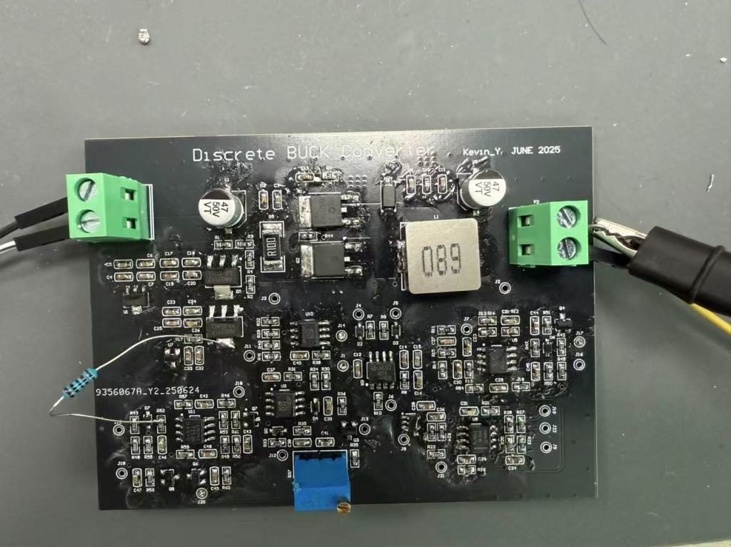
Calculation
Here are equations I used for calculating targeted inductor value, inductor current, and output ripple [1].
Inductor Design Parameter
| Parameter | Value |
|---|---|
| Input Voltage (Vin-max) | 24 V |
| Output Voltage (Vout) | 5 V |
| Switching Frequency (f) | 150 kHz |
| Output Current (Iout) | 2 A |
| Current Ripple Ratio (r) | 0.3 |
| Inductor Ripple Current (ΔIL) | 2.3 A |
| Inductance (L) | 43.98 µH |
| Inductor Saturation Current | 2.76 A |
Input/Output Capacitor Parameters
| Parameter | Value |
|---|---|
| Output Capacitance (Cout) | 80 µF |
| Output Cap ESR | 5 mΩ |
| Output Voltage Ripple (ΔVout) | 9.25 mV |
| Output Ripple Percentage | 0.2% |
| Output Cap Voltage Rating (Vmax) | 7.5 V |
| Input Capacitance (Cin) | 57 µF |
| Input Cap ESR | 5 mΩ |
| Input Voltage Ripple (ΔVin) | 7.31 mV |
Diode Parameters
| Parameter | Value |
|---|---|
| Output Current (Iout) | 2 A |
| Minimum Duty Cycle (Dmin) | 20.83% |
| Average Diode Current (Imax-avg) | 1.9 A |
| Diode Reverse Voltage Rating | 36 V |
Component Selection
Main Power Loop

Schottky diode
Fast switching
Reverse voltage rating > Vcc
Average rectifying current > maximum inductor current during freewheeling (2.76A)
Triangular Wave Generator

| Parameter | Value |
|---|---|
| Vout1 Max | 8 |
| Vout1 Min | 0 |
| Vout2 Max | 8 |
| Vout2 Min | 0 |
| R1 (kΩ) | 100 |
| R2 (kΩ) | 20 |
| Divider V+ | 1.24 |
| V⁺ Min | 1.3333 |
| V⁺ Max | 6.6667 |
| Vmax (Triangle Wave Peak) | 1.488 |
| Vmin (Triangle Wave Valley) | -0.112 |
| Midpoint Voltage | 0.688 |
| Limit Resistor (kΩ) | 5.1 |
| Differentiating Capacitor (µF) | 0.001 |
| Bias Voltage (V) | 3.3 |
| Rise Time (ms) | 0.002472727 |
| Fall Time (ms) | 0.00173617 |
| Triangle Wave Frequency (kHz) | 237.592 |

Why I chose TLV3201 comparator over a normal op-amp
The switching frequency is 237 kHz, meaning the triangle wave edges rise within ~2.1 µs. To generate a clean PWM signal, the comparator must respond quickly to these edge transitions.
I selected the TLV3201, which only offers a 40 ns propagation delay, which is ~50× faster than the triangle’s slope time. That means it easily catches the moment when the control voltage crosses the triangle. In contrast, general-purpose op-amps like the LMV358 may be too slow to respond.
Compensation
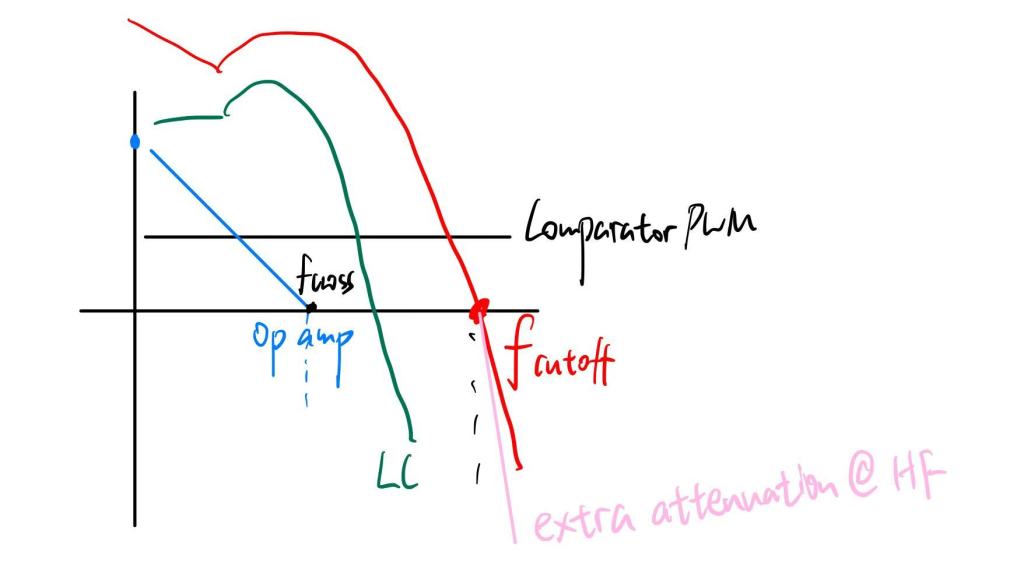
Why We Need Compensation
In a voltage-mode controlled buck converter, the power stage (mainly the LC filter) introduces a double pole at the resonant frequency:
This results in a -180° phase shift near the crossover frequency, turning the loop feedback from negative to positive.
Additionally, the error amplifier contributes its own phase lag, especially when configured as an integrator (normally 90°).
Type III error amplifier topology
This design adopts the Type III error amplifier topology, following a well-established compensation structure from Texas Instruments’ reference designs [2]. The Type III compensator provides:
- Two zeros to cancel LC double poles.
- Two high-frequency poles to suppress noise and handle ESR effects.
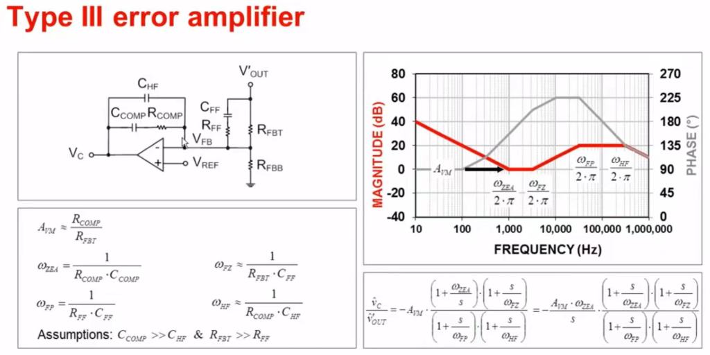
Step 1: Set the System Crossover Frequency
We start by selecting the desired crossover frequency, usually 1/10 of the switching frequency. Then we calculate the integrator pole:

Step 2: Introduce Two Zeros to Compensate LC Double Pole
The LC filter introduces a double pole where there will be a sharp gain drop and phase lag near fLC. To counteract two poles, we add two zeros:
- Zero 1 (Z1) is added by placing a resistor R1 in series with C1 in the feedback path of the op-amp:
- Zero 2 (Z2) is introduced using a series RC network

Why Start by Compensating the Op-Amp Stage First
Op-amp gain is easiest to reduce and dominates at low frequencies. So it is safer to control op-amp first to prevent oscillation.
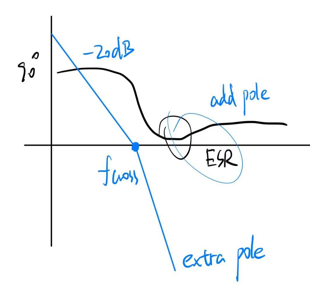
Step 3: Add High-Frequency Poles to Limit Noise and Cancel ESR Zero
- Pole 1 (P₁) is added to cancel the ESR zero introduced by the output capacitor: Real-world capacitors include a small resistance known as ESR (Equivalent Series Resistance). This ESR, combined with the capacitor, forms a zero in the transfer function:

We introduce a pole by adding a Rf2 (<<Rf1) in series with Cf1.
- Pole 2 (P₂) is added at approximately 2× crossover frequency to reduce high-frequency gain and avoid amplifying switching noise.
Design Results and Implementation
Based on the equations and the values selected, the actual loop compensation components are:
| Component | Value Used |
|---|---|
| Rbias | 12 kΩ |
| R1 | 39 kΩ |
| C1 | 4.7 nF |
| R2 | 13 kΩ |
| C2 | 1.2 nF |
| R3 | 13 kΩ |
| C3 | 390 pF |

These component values were chosen based on the results from a spreadsheet calculator referencing the classic design flow in “Switching Power Supplies A–Z Second Edition.” [1]
Frequency Domain Behavior
The following characteristics were achieved:
- Crossover Frequency: 13 kHz
- Zero Placement: Z1 at 2.8 kHz, Z2 at 26 kHz
- Pole Placement: ESR pole at ~195 kHz, P2 at 31 kHz
Our final Bode plot would have:
- Adequate gain roll-off
- A phase margin ~135°, not so well but this didn’t affect the reponse time.
- Clean attenuation of high-frequency noise.
A more detailed compensation
Testing Result
Output with 10Ω Gold Aluminum Resistor Load: 5.22V
With a 12 V input at 0.25 A and a 10 Ω load on the output, the converter bucks the voltage down to 5.22 V.
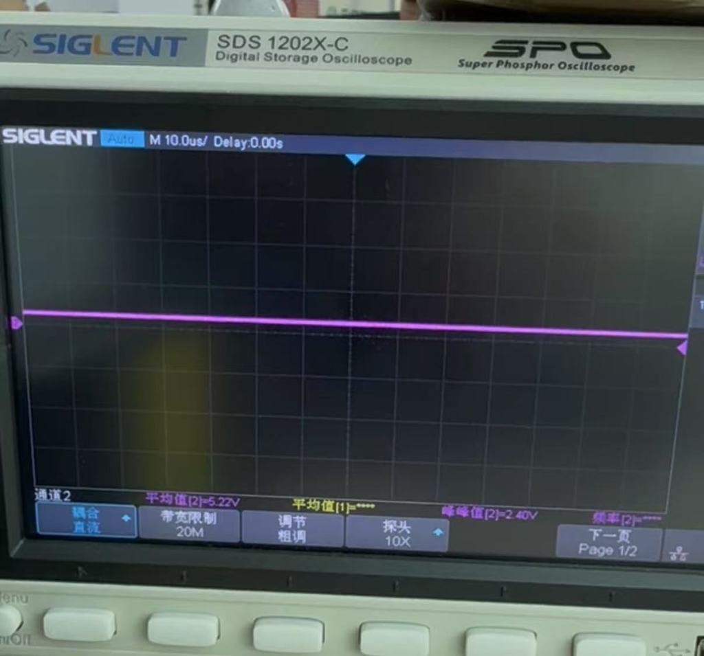
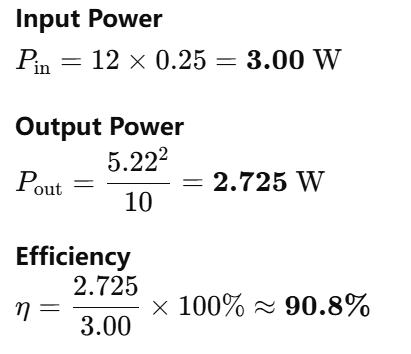
Average Voltage Ripple = 5.63mV: Lower than calculated.

Load Transient Response < 150us
When a sudden load is applied, the output voltage exhibits a brief undershoot but recovers to steady state.
Our own measurements show recovery time under 142 µs, which aligns with the microsecond-level performance demonstrated in a TI’s application report [3].


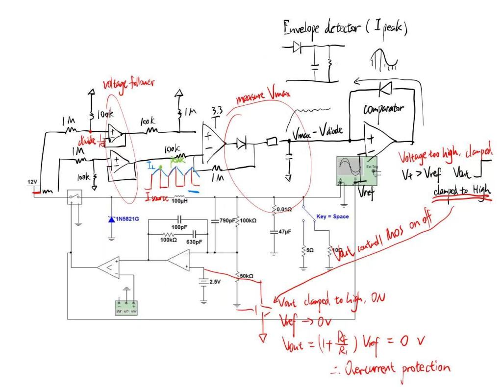
Overcurrent Protection
Through a shunt resistor, voltage across inductor is amplified and peak-detected.
A comparator compares this peak voltage to a reference voltage: when the current is too high, V+ > Vref, then Vout turns high.
The comparator output triggers the MOSFET control logic to short Vref to ground, thereby zeroing out Vout.
Overvoltage Protection

Undervoltage Protection

Overheat Protection

Reference
[1] S. Maniktala, Switching Power Supplies A to Z, 1st ed., Burlington, MA, USA: Newnes (Elsevier), 2006.
[2] R. Sheehan and L. Diana, Switch-mode Power Converter Compensation Made Easy, Texas Instruments, [Online]. Available: https://e2e.ti.com/cfs-file/__key/communityserver-discussions-components-files/196/0412.slup340.pdf.
[3] M. Acanski, Improving Load Transient Response of DC/DC Converters Powering Controlled Loads, Texas Instruments, Application Report SLVAEE0, Sep. 2019.
