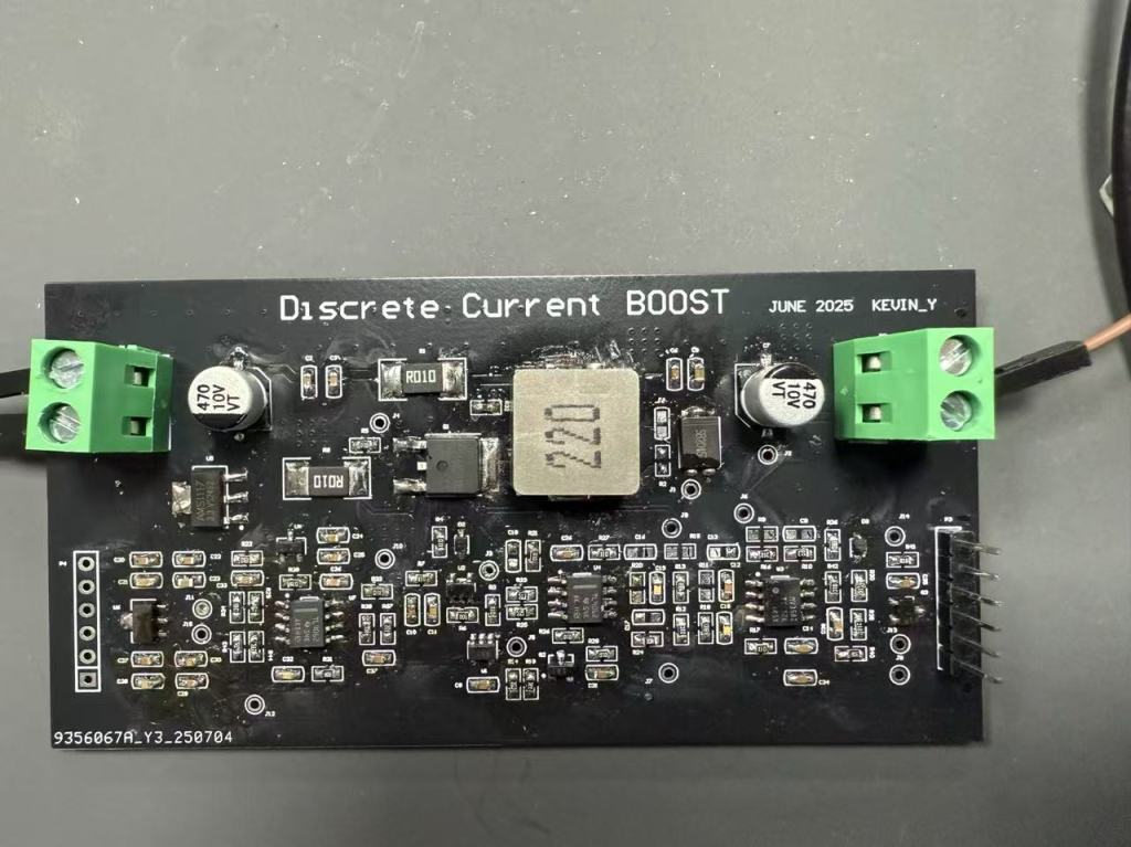
🔹Input Voltage: 5V
🔹Maximum Output Current: 2A
🔹Output Voltage: ~15.4V
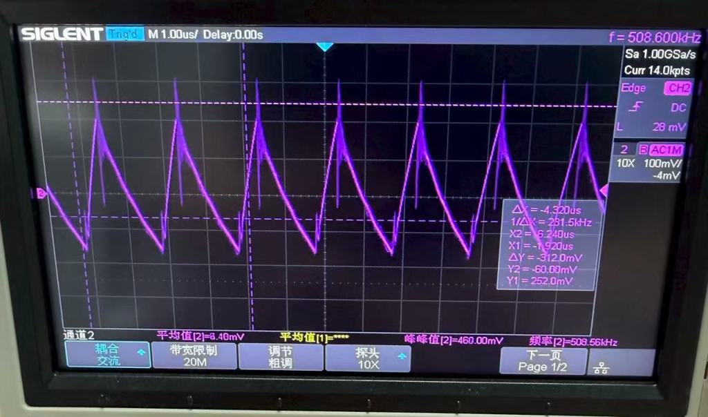
🔹Switching Frequency: ~500 kHz
Regulation & Control Feature
Output Ripple
Load Transient Response
Feedback Loop Compensation
Power Efficiency
Protection Feature
Overcurrent protection
Overheat protection
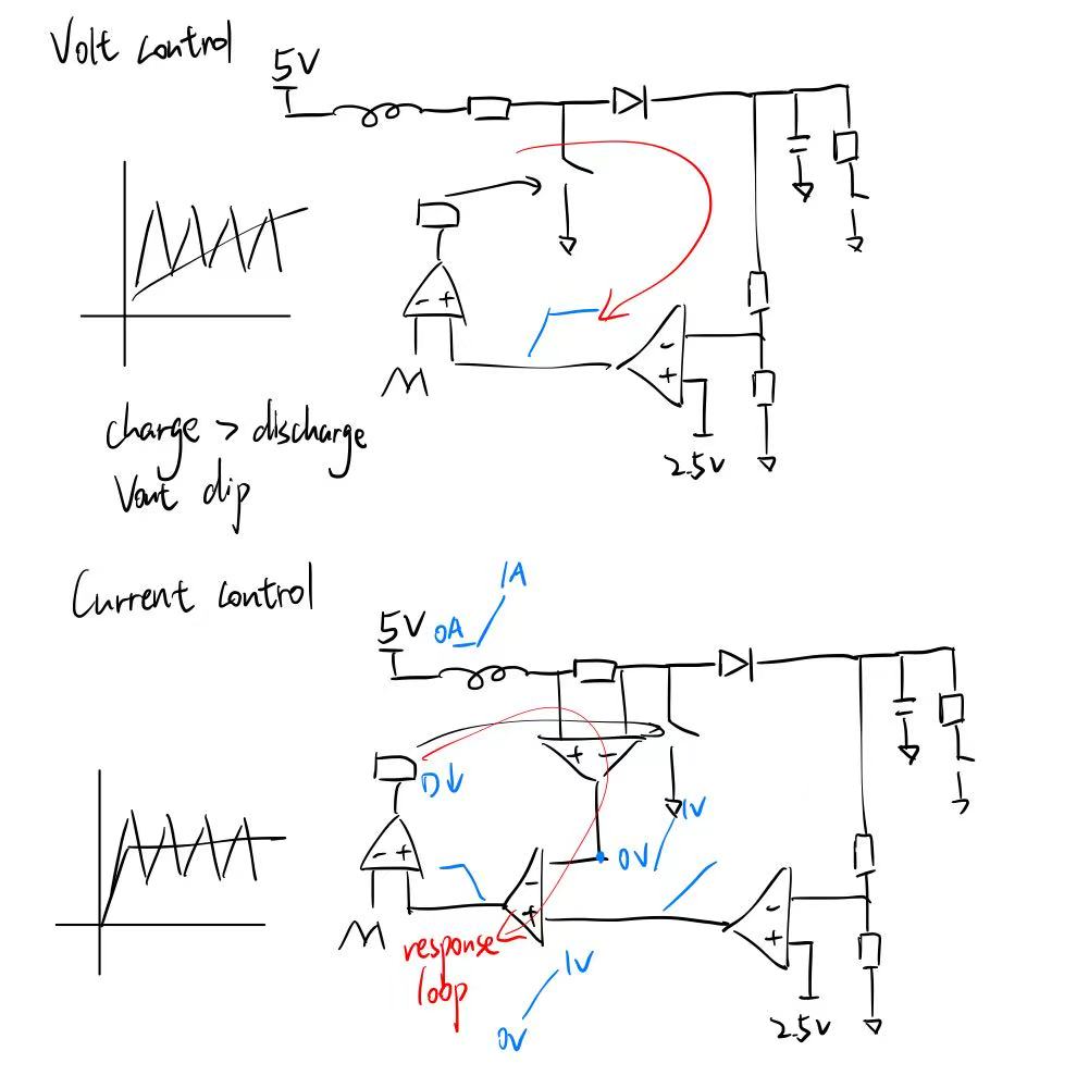
Why Current-Mode Control is Better than Voltage-Mode Control in Boost Converters
One major advantage of current-mode control is that it eliminates the right-half-plane zero (RHPZ) issue found in voltage-mode-controlled boost converters.
This happens because in voltage-mode control when the duty cycle increases, the switch stays on longer, delaying energy transfer to the output.
As a result, the output capacitor discharges further before the inductor delivers energy, causing a temporary drop in Vout. The final rise in output voltage occurs after a delay, thus we observe a noticeable voltage dip before it starts recovering.

However, in current-mode control, we regulate the output voltage indirectly by controlling the inductor current, rather than a slow voltage response.
The controller compares the actual inductor current with a reference current (derived from the voltage error), and this comparison directly determines the switching of the MOSFET.
A more detailed explanation of RHPZ can be found in this YouTube video [1]:
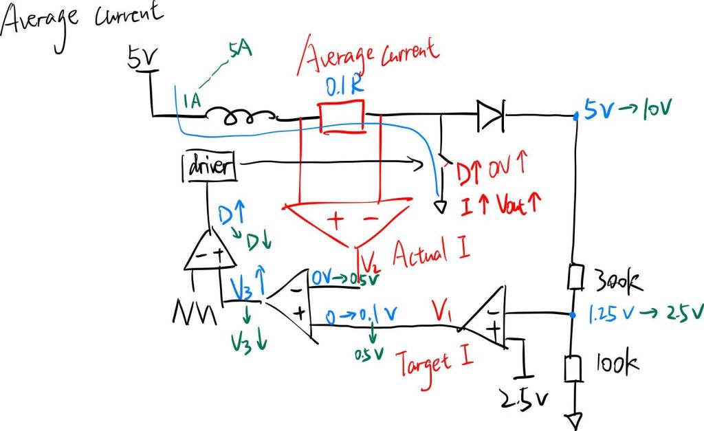
Which Current-Mode Control?
In modern power converter ICs, current-mode control has become the standard. The peak current-mode control is the most commonly used in industry. It often requires additional circuitry like SR latches and sometimes internal dummy load to address oscillation.

However, for my learning purposes, this project intentionally adopts average current-mode control, a more transparent view.
This is done by using a shunt resistor to sense the inductor current. The voltage across this shunt resistor is proportional to the actual current flowing through the inductor. This sensed current is then fed into an error amplifier, where it is compared against a target reference current derived from the output voltage regulation loop.
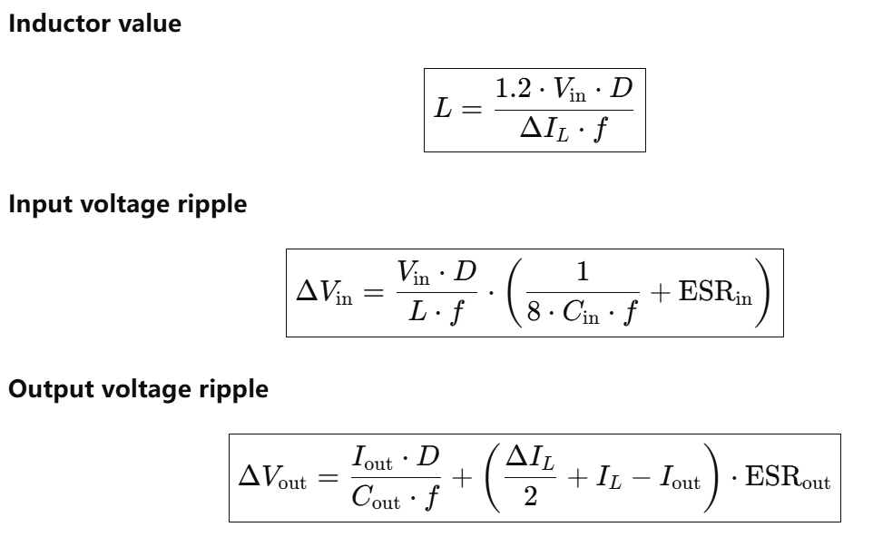
Component Selection
Based on the target input and output specifications, we calculated the average and peak inductor current to select a suitable inductor. Choosing the desired ripple voltage, I can estimate the required input and output capacitance [2].
Basic parameter
| Vin min (V) | Vout max (V) | Duty Cycle D (%) | V diode (V) | Iout (A) | n(%) | Freq (kHz) |
|---|---|---|---|---|---|---|
| 5 | 12 | 59.35 | 0.3 | 2 | 85 | 500 |
Inductor calculation
| Avg IL (A) | ΔIL (A) | IL_peak (A) | L (μH) |
|---|---|---|---|
| 5.788 | 1.736 | 7.988 | 0.171 |
Capacitor and ripple calculation
| Cin (μF) | ESRin (mΩ) | ΔVin (mV) | Cout (μF) | ESRout (mΩ) | ΔVout (mV) |
|---|---|---|---|---|---|
| 470 | 10 | 14.5 | 470 | 50 | 233.0 |
Main Loop

Differential Current Limiting Circuit Design
I sensed inductor current with a 10 mΩ shunt resistor and a TLV9062 differential stage (gain = 2). A diode-BJT network injects a ~0.7 V bias so op-amp offset and startup noise cannot falsely trip the limiter.

A divider from the 3.3 V rail sets VA ≈ 0.87V. When Vout<VA, the loop operates normally; when Vout≥VA the amplifier sinks the COMP (output of the error amplifier) node, reducing duty cycle and limiting peak current.
Compensation
Switching frequency: fsw=500 kHz
Inner current loop: choose fci ≈ fsw/8∼fsw/12 = 40 − 60 kHz
Outer voltage loop: choose fcv ≈ fc/5∼fci/10 = 5 − 10 kHz
On initial power-up I observed a small overshoot at Vout. Diagnosis: the inner current loop was reacting much faster than the outer voltage loop, so the capacitor was briefly over-charged before the outer loop pulled the current command down.
I tuned in two steps:
- Throttle the voltage loop. I increased the COMP integrator capacitor (≈ 1 µF) so the outer loop crosses in the low-kHz range. This prevents the voltage loop from commanding an excessive current step at startup.
- Trim the current loop. I added a small HF capacitor (≈ 1 nF) in the current-sense path to filter switching ripple and slightly lower the current-loop bandwidth, keeping about a 5–10× separation (inner ≫ outer).
Final compensation choice:
- Voltage loop: a Type-II using one capacitor Cc with the gain resistor Rc. Seen by the outer voltage loop—the power stage looks like a current source feeding Rload || Cout

- Given there is one pole, one compensating zero plus an integrator for zero steady-state error is enough.
- Current loop: ≈ 1 nF HF filter to maintain bandwidth separation.
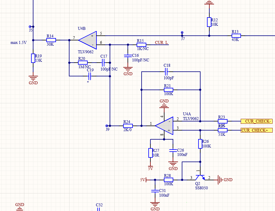
Testing Result
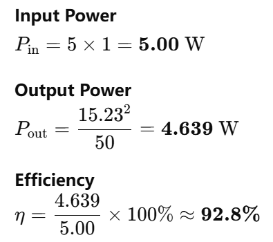
Output with 50Ω Gold Aluminum Resistor Load: 15.23V
With a 5V input at 1 A and a 50 Ω load on the output, the converter boosts the voltage upto 15.23 V.
Average Voltage Ripple = 6.4mV
Load Transient Response < 120us
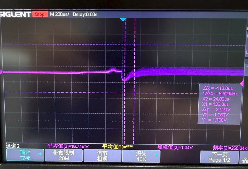

Our own measurements show recovery time under 120 µs, which aligns with the microsecond-level performance demonstrated in a TI’s application report [3].
Reference
[1] S. Ben-Yaakov, “Right Half Plane Zero (RHPZ) in power electronics,” YouTube, Apr. 10, 2018. [Online]. Available: https://www.youtube.com/watch?v=vaU2P1naz8E
[2] S. Maniktala, Switching Power Supplies A to Z, 1st ed., Burlington, MA, USA: Newnes (Elsevier), 2006.
[3] M. Acanski, Improving Load Transient Response of DC/DC Converters Powering Controlled Loads, Texas Instruments, Application Report SLVAEE0, Sep. 2019.
