🔹Input Voltage: 30V
🔹Output Voltage: ~5.4 V
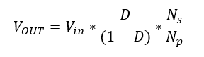
🔹Transformer Turn Ratio: 3:1:2.4
🔹Switching Frequency: ~145 kHz
Design Overview
This design is a buck-mode flyback converter, where the transformer provides isolation and step-down ratio, while the control operates similar to a current-mode boost converter. The PWM comparator compares the sawtooth ramp (V+) with the COMP control voltage (V–). The COMP (V-) node is driven by the TL431 + optocoupler feedback loop, which adjusts duty cycle to regulate the 5 V output.
- With Vout ≈ 0V at startup, the divider node is below 2.5 V and the TL431 is off, so the optocoupler transistor does not conduct. This keeps the V- high, duty cycle increases, and more energy is delivered per cycle, raising Vout.
- As Vout approaches the 5 V target, the divider node reaches 2.5 V, the TL431 begins to conduct, driving current through the optocoupler LED. The optocoupler transistor pulls down the V- of comparator on the primary side, reducing duty cycle and peak current.
In this way, the feedback loop regulates the output voltage: the TL431 sets the reference, while the optocoupler provides galvanic isolation between secondary and primary.


Component Selection
Transformer Turn Ratio
In this design, the turns ratio is constrained by the voltage ratings of both the MOSFET and the output diode. The chart illustrates this relationship:
- The red line represents the MOSFET maximum Vds rating.
- The blue line represents the minimum input voltage requirement.
- The green line shows the diode reverse voltage stress.
- The vertical axis is voltage (V), and the horizontal axis is the turns ratio Np/Ns.
The feasible region is where all constraints overlap. From the plot, the intersection region of the curves points to a practical turns ratio of about 3:1.

Design notes on how large resistors to choose
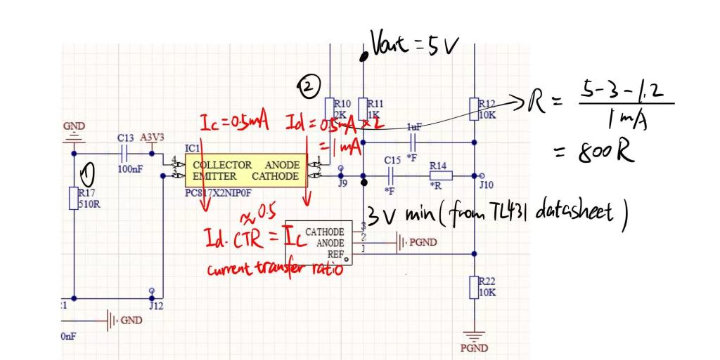
Duty Cycle < 45%, Current Sensing & Scaling
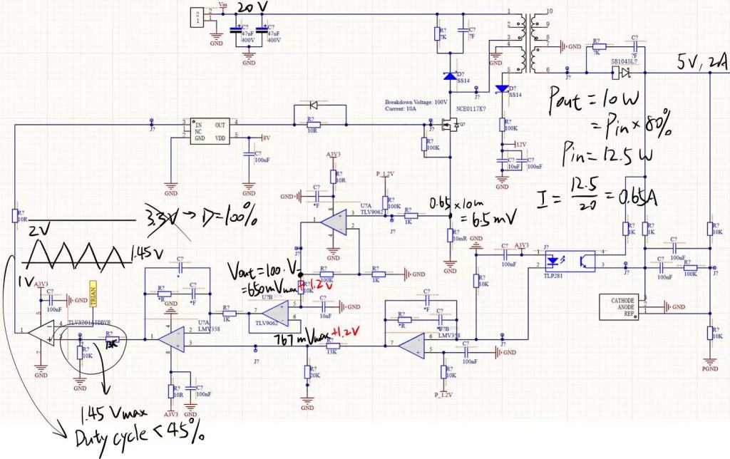
Duty Cycle keeps under 45% considering relations between input and output.
If D is too large (>0.5), the core may not fully reset, and there is little room left when Vin sags or during load transients. If D is too small, ON-time approaches controller limits, efficiency drops, and transient control weakens.
A 10 mΩ shunt resistor yields 10 mV/A with negligible loss; a ×100 TLV9062 stage scales this to 1 V/A, giving a clean 0–2.5 V span for a 0–2.5 A peak limit—perfect for a 3.3 V op amp and simple current limiting.
Rail to rail Op amp LMV358 and TLV9062 (SR, GBP)

1MHz LMV358 is good for 100kHz triangular wave. If the buffered triangular ramp swings from 0–30% of 5 V (≈ 1.5 Vpp) at 100 kHz, the required minimum slew rate is

The LMV358 offers about 0.52 V/µs, which is sufficient for this ramp. An RC network is then added to limit bandwidth.
0.52V/µs is sufficient for LMV358B. For a current slope of 1 A/ms, the 10 mΩ shunt with ×100 gain produces
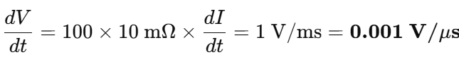
which is far below LMV358’s SR.
The current-sense loop processes the inductor current through a shunt and amplifier, and then takes the average value for regulation. Because this introduces an inherent delay, the current loop requires a higher bandwidth than the outer voltage loop in order to maintain fast response. For this reason I selected the TLV9062, 10MHz rail to rail.
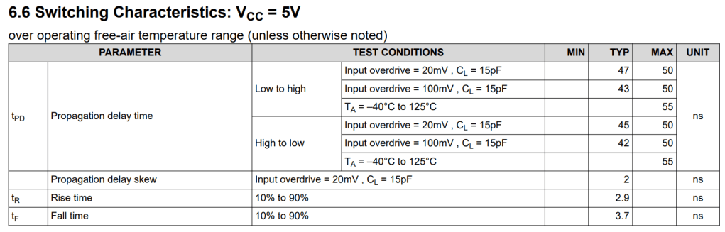
At a switching frequency of 145 kHz (PWM period ≈ 6.9 µs), the comparator must settle much faster than one cycle to avoid duty distortion. Following the common rule of keeping the propagation delay less than 1/10 of the PWM period, the requirement is tpd< 0.69 µs. TLV3201 operates in nano-seconds, therefore meets this requirement [1].
Transformer Winding
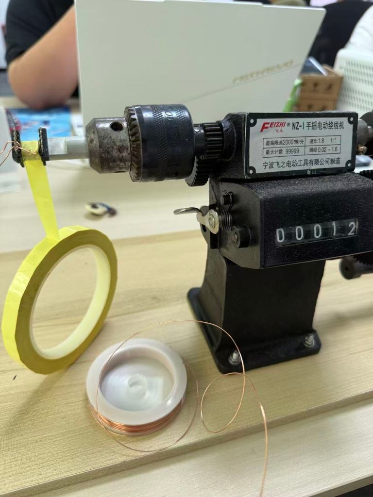
The transformer was designed using calculated parameters from an in-house Excel tool, based on core geometry, inductance requirements, and duty-cycle constraints. The final design uses an EE ferrite core with a gapped structure to achieve the target inductance. The winding configuration was determined as 24 turns primary, 8 turns secondary, and 1 turn auxiliary (12 V), with wire sizes selected to meet current density and skin-effect limits. Design checks verified flux density (<0.3 T), current density, and window utilization factor Ku, so that the transformer operates efficiently without saturation.
Challenges and Solutions
Challenges in the First Flyback Prototype
IIn the first design, using a TLP291 optocoupler caused two problems at startup:
- Audible transformer whine
- Overshoot not suppressed by compensation
The root causes were:
- High CTR of TLP291: The TLP291 has a relatively high CTR, meaning small LED current produces a large collector current on the output side. This makes the feedback loop too sensitive —any small ripple in Vout gets amplified disproportionately.
- Poor transformer coupling, reducing energy transfer.
Fix: I switched to a PC817 (lower CTR) and rewound the transformer with better coupling. This reduced loop gain, and eliminated the whine.
I rewinded the transformer with better coupling and switched to a PC817 optocoupler. With its lower CTR, the loop gain became more controllable, and the output capacitor compensation was now effective.
Challenges in the Second Flyback Prototype
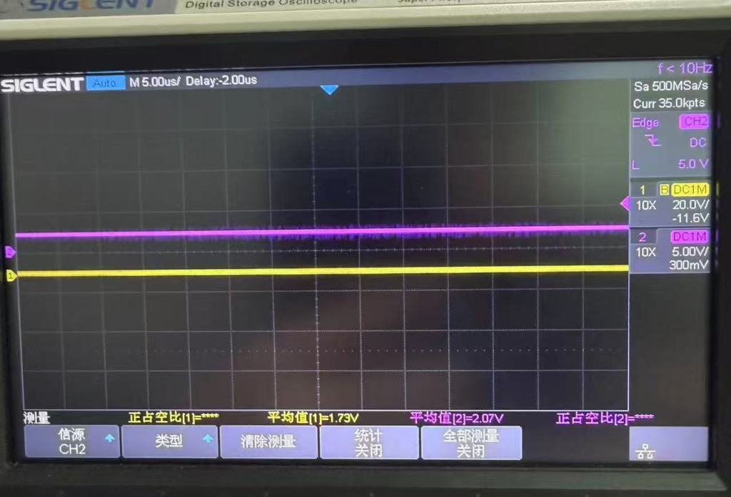
In my second prototype, I kept running into severe output overshoot. After running for a short time, the converter would suddenly shut off, and the transformer emitted audible resonance. At first, I suspected the current loop amplifer running too fast, so I reduced its gain, but the problem persisted.
I probed the optocoupler terminals and discovered that the feedback was too sensitive. Even a small rise in output voltage would drive the optocoupler too strongly, causing the loop to overreact. This created the oscillating overshoot waveform.
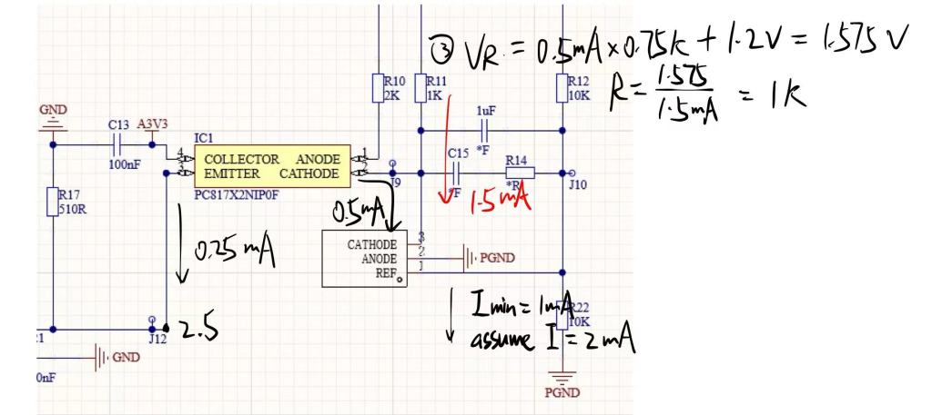
Fix: Reduce the primary-side sense resistor. By requiring more current before the optocoupler LED turns on, the feedback became less sensitive and more stable. As a result, both sides of the optocoupler settled into a smooth conduction waveform.
The figure below confirms that the optocoupler terminals now hold a stable DC value.
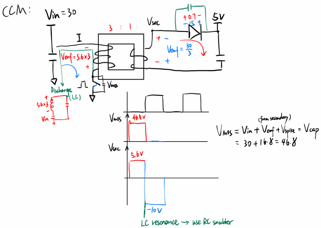
LC Resonance and RC Snubber
One key issue I observed was LC resonance at the diode node, caused by the diode’s junction capacitance and transformer leakage inductance.
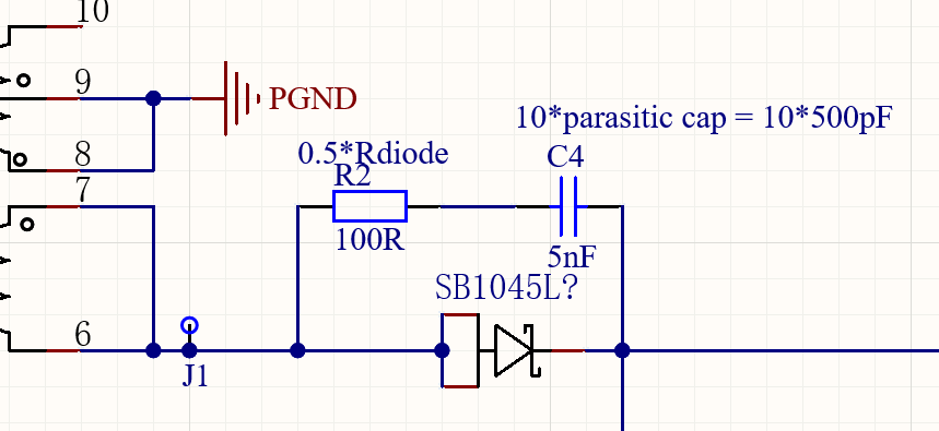
To mitigate this, I added an RC snubber directly across the diode. Following a common design heuristic:
Csnub ≈ 10 × Cparasitic, Rsnub ≈ 0.5 × Rdiode
I selected Csnub = 5 nF and Rsnub = 100 Ω, which effectively damped the resonance.

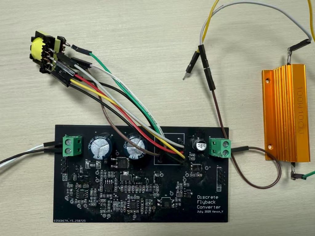
Testing Result
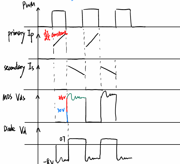
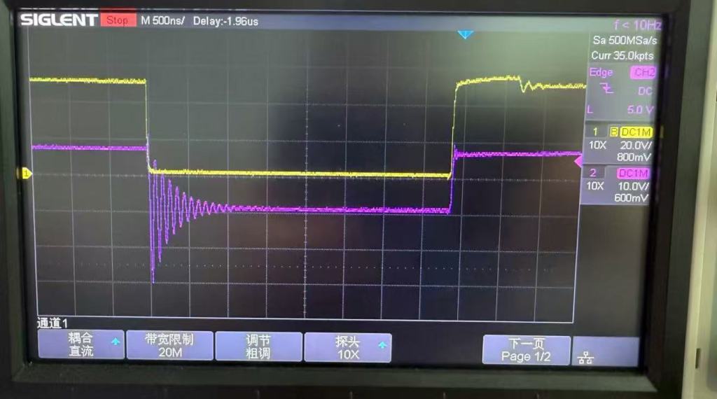
Transformer Node Measurement (CCM)
I measured the voltage across the transformer primary switch (MOSFET drain) and the secondary rectifier diode input. These nodes are the most critical for observing switching behavior and confirming whether the flyback is operating in continuous conduction mode (CCM) as expected.

This aligns with theoretical waveform.
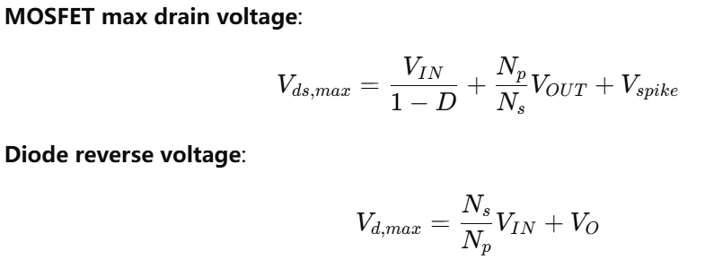
Equations [3]

Reference
[1] Texas Instruments, TLV320x 40ns, microPOWER, Push-Pull Output Comparators (TLV3201, TLV3202), Datasheet SBOS561C, Mar. 2012.
[2] S. Maniktala, Switching Power Supplies A to Z, 1st ed., Burlington, MA, USA: Newnes (Elsevier), 2006.
